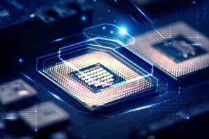
In this blog, we’ll explore the semiconductor fabrication process, step by step—from growing pure silicon crystals to producing integrated circuits (ICs) on tiny wafers. This intricate process involves multiple stages, advanced equipment, and cleanroom environments, where even a speck of dust can ruin a microchip.
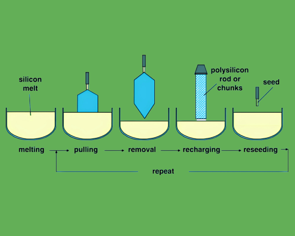
The first step in semiconductor fabrication is the creation of a pure silicon ingot, which will later be sliced into wafers. Silicon, the primary material used in semiconductor manufacturing, is purified from sand (silicon dioxide) in a process known as the Czochralski method.
Melting Silicon:
Ultra-pure silicon is melted at high temperatures.
Crystal Pulling:
A seed crystal is dipped into the molten silicon and slowly pulled upward while rotating, forming a cylindrical single crystal (called a silicon ingot).
Ingot Shaping:
The ingot is then precisely shaped and sliced into thin discs called wafers. These wafers will be the foundation for the semiconductor devices.
Photolithography: Printing Circuit Patterns
What Is Photolithography?
Photolithography is a crucial step in semiconductor fabrication. It’s a process where intricate circuit patterns are “printed” onto the silicon wafer. This step forms the transistors and other electronic components within the semiconductor device.
Process Steps:
Photoresist Coating: The wafer is coated with a light-sensitive material called photoresist.
Mask Alignment: A photomask, which contains the circuit design, is aligned over the wafer.
Exposure: Ultraviolet (UV) light shines through the photomask, exposing the photoresist in the desired pattern.
Development: The exposed photoresist is developed, leaving behind the patterned design on the wafer.
Photolithography enables the creation of features as small as 7 nanometers (nm) in modern processors.
Etching: Removing Unwanted Material
Once the circuit pattern has been created, the next step is to remove unwanted material from the wafer surface through etching. This process carves out the fine details of the circuitry.
Types of Etching:
Wet Etching
Dry Etching (Plasma Etching)
Wet Etching:
Involves using chemicals to dissolve the unprotected material on the wafer surface. While effective, it is less commonly used today because it can lead to less precise edges.
Dry Etching (Plasma Etching):
Uses ionized gases (plasma) to selectively remove material. This method provides highly accurate results, making it ideal for creating the tiny structures found in modern semiconductors.
Doping: Altering Semiconductor Properties
Doping is the process of adding impurities to the wafer to change its electrical properties. This is done in a highly controlled manner to create N-type and P-type regions, essential for forming PN junctions and transistors.
2.Diffusion:
The wafer is heated to allow the dopants to diffuse more evenly into the silicon, creating the desired electrical properties.
How Doping Is Performed:
1. Ion Implantation:
High-energy ions are shot into the wafer, embedding themselves into the semiconductor material.
Types of Deposition:
Chemical Vapor Deposition (CVD):
In this process, a chemical reaction is used to deposit a thin layer of material onto the wafer.
Physical Vapor Deposition (PVD):
This method involves vaporizing a material in a vacuum, which then condenses onto the wafer as a thin film.
Deposition: Building Layers of Material
The next step in semiconductor fabrication is deposition, where thin films of various materials (like insulators or conductive metals) are added to the wafer. These layers are crucial for the electrical functionality of the device.
Why It’s Important:
These deposition layers are used to create the insulators and metal connections necessary for the semiconductor device to function, such as forming the metal lines that connect transistors in an integrated circuit.
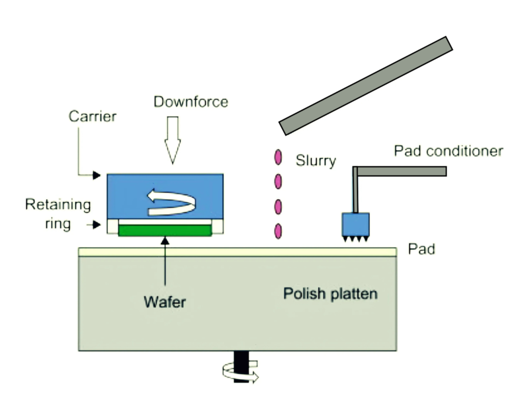
Chemical Mechanical Planarization (CMP): Smoothing the Surface
After multiple layers have been added to the wafer, the surface becomes uneven. Chemical Mechanical Planarization (CMP) is a process used to smooth the surface of the wafer, ensuring that subsequent layers are deposited evenly.
How CMP Works: A slurry of chemicals and abrasive particles is used in conjunction with mechanical polishing to flatten the surface of the wafer.
This step is critical in ensuring that the wafer is perfectly flat, which is essential for creating functional microchips with multiple layers of circuits.
Metallization: Creating Electrical Connections
Metallization is the process of adding metal layers to the wafer to form the electrical connections between different components on the chip. This step turns the wafer into a functioning electronic device by connecting transistors, resistors, and capacitors.
Metals Used:
Aluminum and Copper are commonly used due to their excellent conductivity.
After the metal is deposited, the wafer undergoes another photolithography process to pattern the metal into the appropriate circuit connections.
Packaging and Testing: Final Steps Before Shipping
Once the semiconductor device is fully fabricated, it undergoes packaging and testing.
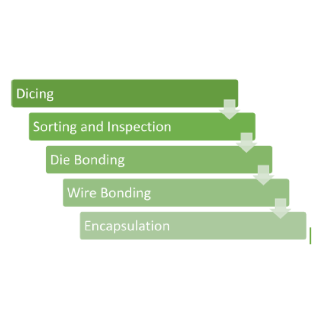
Packaging:
The wafer is diced into individual chips, and each chip is placed in a protective package. This package provides the electrical connections that allow the chip to interface with external devices, such as a motherboard or phone circuit board.
Dicing
Cutting the wafer into individual chips
Sorting and Inspection
Checking chips for defects and sorting them
Die Bonding
Attaching the chip onto a substrate or package base
Wire Bonding
Connecting the chip to external leads using thin wires
Encapsulation
Sealing the chip with protective material (e.g., resin or plastic)
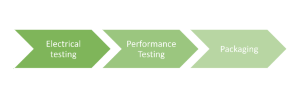
2. Testing: Each chip undergoes rigorous testing to ensure it meets the required performance standards. Only functional chips are shipped to be used in electronic devices.
Electrical Testing
Verifying the chip’s basic functionality through electrical tests
Performance Testing
Ensuring the chip meets required performance metrics
Electrical Testing
Verifying the chip’s basic functionality through electrical tests
Conclusion
The semiconductor fabrication process is a complex and highly detailed journey from raw silicon to advanced microchips, involving many intricate steps like photolithography, doping, and metallization. Each stage must be carefully controlled to ensure the final product meets the exacting standards of modern technology. This process is fundamental to producing everything from the processors in our computers to the solar cells powering the green energy revolution.
In the next blog, we’ll explore the exciting applications of semiconductors, looking at how these components are used in consumer electronics, the automotive industry, telecommunications, and renewable energy solutions.


")
")