Semiconductor devices, from simple diodes to advanced integrated circuits, rely on a deep understanding of physics. Without a grasp of how electrons move, energy bands, and the formation of PN junctions, it’s difficult to appreciate how semiconductors function at a microscopic level. In this blog, we’ll dive into the fundamental physics that govern the behavior of semiconductors and make them the backbone of modern technology.
In solid-state physics, the energy levels of electrons are grouped into bands. Understanding the concept of energy bands is critical to comprehending how semiconductors differ from conductors and insulators.
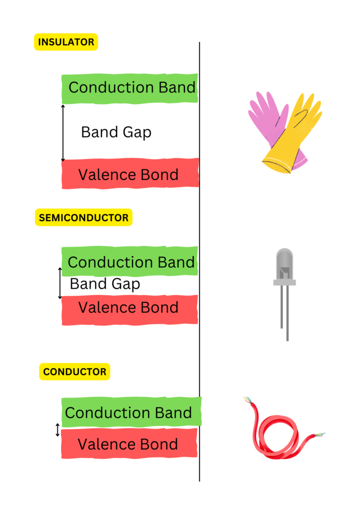
Energy Band Structure:
Valence Band: The energy band where electrons are bound to atoms, making them unavailable for conduction.
Conduction Band: The energy band where electrons are free to move through the material, allowing them to conduct electricity.
Band Gap: The energy gap between the valence band and the conduction band. This gap determines whether a material behaves as a conductor, semiconductor, or insulator.
In Semiconductors:
The band gap in semiconductors is small enough (~1-1.5 eV for silicon) that electrons can jump from the valence band to the conduction band when energy is applied (e.g., heat, light, or electrical voltage). This allows semiconductors to conduct electricity under the right conditions.
Charge Carriers: Electrons and Holes
In semiconductors, electrical current is carried by two types of charge carriers: electrons and holes.
How Current Flows in Semiconductors:
Current in a semiconductor is the result of both electrons and holes moving in opposite directions. In N-type materials, electrons move from the negatively charged terminal toward the positive, while in P-type materials, holes move toward the negative terminal.
Electrons as Charge Carriers:
Electrons in the conduction band are free to move and conduct electricity. These negatively charged particles are the primary carriers in N-type semiconductors, which have been doped to increase the number of free electrons.
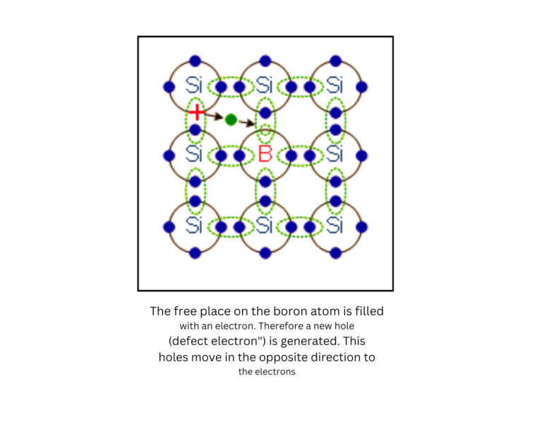
Holes as Charge Carriers:
A hole is essentially the absence of an electron in the valence band. When an electron moves, it leaves behind a “hole,” which behaves like a positive charge. In P-type semiconductors, the movement of these holes contributes to current flow.
Doping: Engineering the Properties of Semiconductors
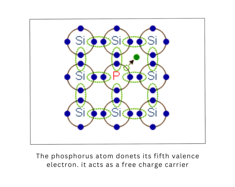
N-type Doping:
In N-type semiconductors, elements with extra electrons (such as phosphorus or arsenic) are added to silicon. These extra electrons become free to move in the conduction band, increasing the semiconductor’s conductivity.
P-type Doping:
In P-type semiconductors, elements like boron or gallium are added. These atoms have fewer electrons, which creates “holes” in the semiconductor’s structure. These holes act as positive charge carriers and move through the material when a current is applied.
PN Junction: The Heart of Semiconductor Devices
The PN junction is one of the most important concepts in semiconductor physics. It is formed when a P-type and an N-type semiconductor are joined together. This junction is the foundation of many semiconductor devices, such as diodes and transistors.
Applications of PN Junctions:
Diodes: A PN junction diode allows current to flow in one direction only, making it useful for converting AC to DC in power supplies.
Solar Cells: In solar cells, PN junctions help convert light into electrical energy by separating electron-hole pairs generated by sunlight.
How a PN Junction Works:
At the junction of the P-type and N-type materials, electrons from the N-side diffuse into the P-side, and holes from the P-side diffuse into the N-side. This creates a depletion region where there are no free charge carriers.
In forward bias (positive voltage applied to the P-side), the depletion region becomes narrower, allowing current to flow across the junction. In reverse bias (positive voltage applied to the N-side), the depletion region widens, preventing current from flowing.
Semiconductor Materials and Temperature Sensitivity
Semiconductors are highly sensitive to temperature, and their conductivity changes with temperature.
Why Silicon Is Preferred:
Silicon, the most widely used semiconductor material, has a relatively moderate band gap (~1.1 eV), making it stable under varying temperatures and highly efficient for most electronic applications.
Thermal Excitation:
As temperature increases, more electrons gain enough energy to jump from the valence band to the conduction band, increasing the semiconductor’s conductivity.
This sensitivity makes semiconductors ideal for temperature sensors and other thermally-sensitive applications.
Key Formulas in Semiconductor Physics
To better understand semiconductor behavior, here are a few key formulas used in semiconductor physics:
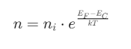
Electron Concentration
Where:
ni is the intrinsic carrier concentration
EF is the Fermi level
EC is the conduction band energy
k is the Boltzmann constant
T is the temperature
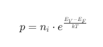
Hole Concentration
Where:
EV is the valence band energy
Drift Current
Where:
q is the electron charge
un is the electron mobility
n is the carrier concentration
E is the electric field
Conclusion
Semiconductor physics is the foundation of all modern electronic devices. Concepts like energy bands, charge carriers, and PN junctions not only explain how semiconductors work, but also enable the creation of advanced technologies such as transistors, diodes, and solar cells. Understanding these principles is key to appreciating how semiconductors have shaped—and continue to shape—the world we live in.
In the next blog, we’ll take a closer look at the semiconductor fabrication process, exploring how these materials are turned into functional devices through intricate manufacturing techniques.


")
")